BJT and FET Working construction
In this article we will learn about the BJT and FET working construction . will also discuss about the basic working of Transistor.
Transistor Working construction
Transistor is a semiconductor device. I is used as to amplify the signals and switch to electronic and electrical signal and power. Generally it has three terminals (legs) to connect in circuit.
1.Terminal-1 is Base:
This is responsible for activating the transistor
2. Terminal-2 is collector:
This is the positive terminal.
3. Terminal-3 is Em miter:
This is the negative terminal of transistor.
Transistor is very small in size and very efficient in work. Its operation is very safe because of its operation is on very low voltages.
Types of Transistor
Transistor is mainly of two type ; bipolar junction transistor (BJT) and filed effect transistor (FET).
- Field effect Transistor (FET)
- Bipolar Junction Transistor (BJT)
BJT And FET Working Construction
1. Bipolar Junction Transistor (BJT) Working Construction
transistor is a 3 layer semiconductor device. The em miter is heavily doped, base is lightly doped the collector only lightly doped. Outer layer width is much greater than those of sandwiched p on n-type material. For transistor the ratio of width of outer layer to that of sandwiched p or n type material is (150:1). Doping of the sandwiched layer is less than that of outer layer. this lower doping level decrease the conductivity of this material by limiting the number of free electrons. the term bipolar reflects the fact that holes and electrons participate in the injection process in to the oppositely polarized material
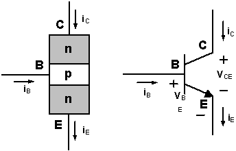
For proper biasing base emitter loop is forward biased and base collector loop is Reverse Biased . the depletion has been reduced in width the due to the applied bias between emitter and base resulting in a heavy flow of majority carriers from P to the n-type material. Due to reverse bias between base and collector the depletion with has been increased and the flow of majority carrier is zero, resulting in only a minority carrier flow. when there is both forward biased and reverse Biased a large number of majority carrier will diffuse across the forward bias PN junction into n type material. since Sandwiched and n-type material is very thin and has low conductivity a very small number of flux career will take path of high resistance to the base terminal.
a large number of majority carriers diffuse across the reverse bias junction into the p-type material connected to the collector terminal,the reason for the relative case with which the majority carriers can cross the reverse bias is easily understood if we considered that for the reverse bias diode the injected majority career will appear as a majority carrier in the n-type material.
IE= IC+ IB
2. Field Effect Transistor Working Construction
Field effect transistor just as a PNP and NPN bipolar junction transistor, there are n channel and p channel field effect transistors. Field effect transistor is an unipolar device. For FET, an electric field is established by charge present that will control the conduction path of the output without the need for direct contact between the controlling and control quantities.
![]()
FET most characteristic is it has high impedance input. BJT outputs are more sensitive to change in input quantities while FET output is less sensitive to change in input quantities.
Hence these are BJT and FET working construction . if you will find any incorrect in above article please comment below in comment box.
If you want to know more about the BJT and FET working construction you must watch this video.